- 您现在的位置:买卖IC网 > Sheet目录1992 > CYW305OXC (Silicon Laboratories Inc)IC CLOCK W305 SOLANO 56SSOP
W305B
........................ Document #: 38-07262 Rev. *B Page 7 of 20
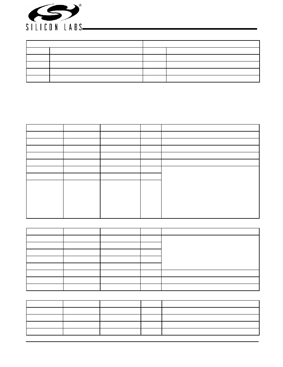
W305B Serial Configuration Map
The serial bits will be read by the clock driver in the following
order:
Byte 0 – Bits 7, 6, 5, 4, 3, 2, 1, 0
Byte 1 – Bits 7, 6, 5, 4, 3, 2, 1, 0
Byte N – Bits 7, 6, 5, 4, 3, 2, 1, 0
All unused register bits (reserved and N/A) should be written
to a “0” level.
All register bits labeled “Initialize to 0” must be written to zero
during initialization.
29
Acknowledge from slave
30:37
Data byte from slave – 8 bits
38
Not Acknowledge
39
Stop
Table 4. Byte Read and Byte Write Protocol (continued)
Byte Write Protocol
Byte Read Protocol
Bit
Description
Bit
Description
Byte 0: Control Register 0
Bit
Pin#
Name
Default
Description
Bit 7
-
SEL4
0
See Table 5
Bit 6
-
SEL3
0
See Table 5
Bit 5
-
SEL2
0
See Table 5
Bit 4
-
SEL1
0
See Table 5
Bit 3
-
SEL0
0
See Table 5
Bit 2
-
Spread Select2
0
‘000’ = Normal (spread off)
‘001’ = Test Mode
‘010’ = Reserved
‘011’ = Three-Stated
‘100’ = –0.5%
‘101’ = ±0.5%
‘110’ = ±0.25%
‘111’ = ±0.38%
Bit 1
-
Spread Select1
0
Bit 0
-
Spread Select0
0
Byte 1: Control Register 1
Bit
Pin#
Name
Default
Description
Bit 7
23
Latched FS4 input
X
Latched FS[4:0] inputs. These bits are read only.
Bit 6
3
Latched FS3 input
X
Bit 5
13
Latched FS2 input
X
Bit 4
12
Latched FS1 input
X
Bit 3
11
Latched FS0 input
X
Bit 2
-
Reserved
0
Reserved
Bit 1
3
REF2X
1
(Active/Inactive)
Bit 0
-
Reserved
0
Reserved
Byte 2: Control Register 2
Bit
Pin#
Name
Default
Description
Bit 7
20
PCI7
1
(Active/Inactive)
Bit 6
19
PCI6
1
(Active/Inactive)
Bit 5
18
PCI5
1
(Active/Inactive)
Bit 4
16
PCI4
1
(Active/Inactive)
发布紧急采购,3分钟左右您将得到回复。
相关PDF资料
DAC5674IPHPG4
IC DAC 14BIT 400MSPS 48-HTQFP
DAC7621EBG4
IC SNGL 12BIT PARALLEL D/A 20SSO
DAC7801KPG4
IC DUAL 12BIT CMOS DAC 24-DIP
DAC8043AESZ
IC DAC 12BIT MULT SRL INP 8SOIC
DAC8043GP
IC DAC 12BIT MULTIPLY CMOS 8-DIP
DAC8221GP
IC DAC 12BIT DUAL W/BUFF 24-DIP
DAC8222GPZ
IC DAC 12BIT DUAL W/BUFF 24DIP
DAC8229FSZ-REEL
IC DAC 8BIT DUAL V-OUT 20SOIC
相关代理商/技术参数
CYW305OXCT
功能描述:时钟发生器及支持产品 Legacy-Sys Clk Intel RSolano Chip W305B RoHS:否 制造商:Silicon Labs 类型:Clock Generators 最大输入频率:14.318 MHz 最大输出频率:166 MHz 输出端数量:16 占空比 - 最大:55 % 工作电源电压:3.3 V 工作电源电流:1 mA 最大工作温度:+ 85 C 安装风格:SMD/SMT 封装 / 箱体:QFN-56
CYW311OXC
功能描述:时钟发生器及支持产品 Sys Clk VIATM Pro266 DDR Chipset W311 DS RoHS:否 制造商:Silicon Labs 类型:Clock Generators 最大输入频率:14.318 MHz 最大输出频率:166 MHz 输出端数量:16 占空比 - 最大:55 % 工作电源电压:3.3 V 工作电源电流:1 mA 最大工作温度:+ 85 C 安装风格:SMD/SMT 封装 / 箱体:QFN-56
CYW311OXCT
功能描述:时钟发生器及支持产品 Sys Clk VIATM Pro266 DDR Chipset W311 DS RoHS:否 制造商:Silicon Labs 类型:Clock Generators 最大输入频率:14.318 MHz 最大输出频率:166 MHz 输出端数量:16 占空比 - 最大:55 % 工作电源电压:3.3 V 工作电源电流:1 mA 最大工作温度:+ 85 C 安装风格:SMD/SMT 封装 / 箱体:QFN-56
CYW312OXC
制造商:SPECTRALINEAR 制造商全称:SPECTRALINEAR 功能描述:FTG for VIA⑩ K7 Series Chipset with Programmable Output Frequency
CYW312OXCT
制造商:CYPRESS 制造商全称:Cypress Semiconductor 功能描述:FTG for VIA⑩ K7 Series Chipset with Programmable Output Frequency
CYW320OXC-3
功能描述:时钟合成器/抖动清除器 Legacy, W320-03 datasheet RoHS:否 制造商:Skyworks Solutions, Inc. 输出端数量: 输出电平: 最大输出频率: 输入电平: 最大输入频率:6.1 GHz 电源电压-最大:3.3 V 电源电压-最小:2.7 V 封装 / 箱体:TSSOP-28 封装:Reel
CYW320OXC-3T
功能描述:时钟合成器/抖动清除器 Legacy, W320-03 datasheet RoHS:否 制造商:Skyworks Solutions, Inc. 输出端数量: 输出电平: 最大输出频率: 输入电平: 最大输入频率:6.1 GHz 电源电压-最大:3.3 V 电源电压-最小:2.7 V 封装 / 箱体:TSSOP-28 封装:Reel
CYW320OXC-4
功能描述:时钟合成器/抖动清除器 Legacy, W320-04 datasheet RoHS:否 制造商:Skyworks Solutions, Inc. 输出端数量: 输出电平: 最大输出频率: 输入电平: 最大输入频率:6.1 GHz 电源电压-最大:3.3 V 电源电压-最小:2.7 V 封装 / 箱体:TSSOP-28 封装:Reel